I’ve been working on designing and building a MIDI synthesizer (called the ApOPL3xy) based on the OPL3 FM synthesis chip and the ATmega1284 microcontroller. I’ve made a couple of posts about it (here and here) and have gotten some good questions from some people about how this or that works under the hood. So, for this post, I thought I’d dig a little deeper into the technical details. I’ll go over the various components and how they’re connected together. If needed, I may make other posts focusing on some of the components in further detail.
Microcontroller
The microcontroller that drives the system is the Microchip ATmega1284. (It used to be made by Atmel, before Microchip bought them.) The ATmega1284 is an 8-bit AVR microcontroller, similar to but more powerful than the ATmega328P at the heart of the Arduino Uno R3.
Hardware
Chips in the AVR line of microcontrollers have integrated flash memory for storing programs, SRAM for program variables and stack, and an EEPROM for non-volatile data storage. Most have hardware implementations of several communication protocols, such as SPI, I2C, and TTL Serial (basically RS-232 but with different voltage levels).
Whereas the ATmega328P has 32 kB of flash, 2 kB of SRAM, and 1 kB of EEPROM, the ATmega1284 has 128 kB of flash, 16 kB of SRAM, and 4 kB of EEPROM. I had initially designed the ApOPL3xy around the ATmega328P, but soon found the memory constraints too limiting, especially the 2 kB of SRAM. So, I upgraded to the ATmega1284. 128 kB of program flash and 16 kB of on-chip SRAM should be more than enough for the initial version, and leave plenty of room for future expansion.
The microcontroller in the ApOPL3xy runs at 5V and 20 MHz. A quartz crystal is used to generate the clock signal. 20 MHz is the maximum clock frequency for which the ATmega1284 is rated, and so far, it seems to be sufficient.
Programming
Arduino boards each have a USB port connected to a USB-to-serial bridge chip, which is used by special bootloader code on the microcontroller to receive new program code, so that all one needs to program an Arduino is a USB cable. When using a bare microcontroller as the ApOPL3xy does, the way to program it is ISP (In-circuit Serial Programming), sometimes called ICSP. This uses the SPI bus to upload code to the microcontroller (configured as the slave). However, to do this, one needs a separate device to act as the SPI master and upload the code to the microcontroller. I’m using the AVRISP-mkII programmer for this project. There are many others, but I have read that some of them have trouble with chips that have more than 64 kB of flash. I have, so far, not had any problems with the AVRISP-mkII, but note that the compiled firmware is still less than 64 kB in size, so that’s not entirely conclusive.
I’m using the PlatformIO IDE to edit, compile, and upload code to the microcontroller. This could be done with the official Arduino IDE as well (with the MightyCore board definitions added), and I was doing it that way for a while. However, the Arduino IDE is not very developer-friendly for large projects, and it makes simple things like having multiple source files much more difficult than they should be. PlatformIO, on the other hand, is much easier to use and I find myself fighting with it much less than with the Arduino IDE. PlatformIO is a Visual Studio Code extension, so you’ll need that installed, but it’s cross-platform, supports a large number of microcontrollers, and can use libraries written for the Arduino IDE. In theory, it even supports debugging over JTAG if the chip supports it. I haven’t tried that yet, but the ATmega1284 does claim to support it. PlatformIO is still a tad rough around the edges, but it’s so much better than the Arduino IDE experience that I highly recommend it.
Peripheral Devices
The ApOPL3xy has several peripheral devices attached to the microcontroller. “Peripheral” here means that the device is separate from the microcontroller chip, not necessarily that it’s detachable from the circuit board. Each of these peripherals communicates with the microcontroller using the SPI protocol. The one exception to this is the MIDI input port, which communicates using TTL Serial and is therefore connected to one of the microcontroller’s USART (i.e. hardware serial) interfaces.
The ApOPL3xy contains the following peripheral devices:
- OPL3 FM synthesis chip (Yamaha YMF262)
- 20×4 LCD character display module (with Hitachi HD44780-compatible controller)
- Input controls
- 2 EC11 incremental rotary encoders
- 10 tactile push buttons
- MicroSD card module
- 128 kB SRAM (Microchip 23LCV1024)
- 128 kB EEPROM (Microchip 25AA1024)
- MIDI 5-pin DIN input port
- I’m thinking about adding a MIDI thru port as well
- Reset button
Reset Circuit
The reset button is connected to the reset pins of both the ATmega1284 and the OPL3. Since this signal is not being handled by a GPIO pin, software debouncing is not really an option. I also wanted the reset signal to start out active, so that the chips connected to it would be reset at power on. So, I designed a simple RC (resistor-capacitor) circuit, with its analog output converted to digital by means of two gates from a 74HC14 (six Schmitt-trigger inverters).
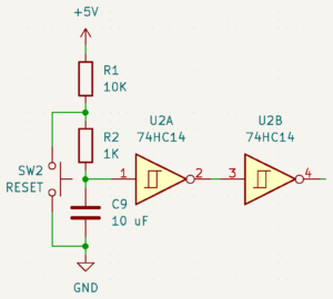
The reset signal for both chips is active low (as it is for most chips with a reset pin), so the way this circuit works is as follows. One lead of a 10 μF capacitor is connected to GND (0V), so the other lead starts out at 0V as well. The second lead is connected to VCC (+5V) through a 10kΩ resistor and a 1kΩ resistor in series, so the capacitor gradually charges to +5V over time. After about 60 ms, the voltage at the second lead becomes high enough to trigger the first inverter, which goes low, and then the second inverter goes high, deactivating the reset signal.
When the reset button is pressed, it connects the second lead of the capacitor to ground through just the 1kΩ resistor, allowing it to discharge quickly, bringing the reset signal low (active). The signal stays low until the reset button is released, at which time, it takes about another 60 ms for the capacitor to charge up enough to bring the reset signal high again. If the button bounces when pressed, that high frequency oscillation is filtered out by the slow-charging capacitor, which is acting as a low-pass filter.
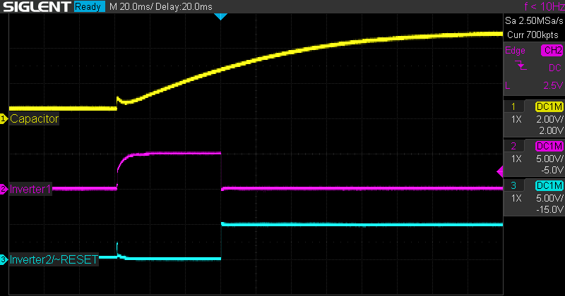
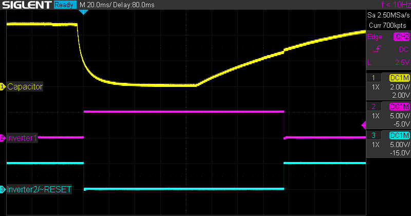
Here are a couple of captures from my oscilloscope illustrating the behavior of the circuit. In these images, the yellow trace measures the voltage across the capacitor, the pink trace measures the output of the first inverter, and the blue trace measures the output of the second inverter, which is the reset signal itself. The first image shows the behavior as the system is powered on. You can see the capacitor charging and how the schmitt-trigger inverters react to it.
The second image shows the behavior when the reset button is pressed. In this capture, you can see the capacitor quickly discharging as soon as the button is pressed, and remain discharged until the button is released, then start slowly charging again.
Custom SPI Interface
Three of the peripherals (MicroSD, SRAM, EEPROM) connected to the microcontroller natively communicate using SPI. The others do not, but in order to conserve GPIO pins, I built an SPI interface for them (except for the MIDI port) using shift registers. In a recent post, I described how this works in more detail. I could have used something a bit fancier, like the Microchip MCP23S17 SPI I/O expander. But they’re more expensive and more proprietary than standard 74HC shift registers, and the shift registers work just fine.
The SPI interface is built from one 74HC595 (serial-in / parallel-out shift register), two 74HC165‘s (parallel-in / serial-out shift registers), and one gate each from a 74HC14 and a 74HC125 (four tri-state buffers). I could have used a 74HC04 instead of a 74HC14, as I’m not using the Schmitt trigger functionality, but I already had a 74HC14 in the design for the reset button circuit, and I wasn’t using all of its gates. This setup provides eight output pins and sixteen input pins, and uses only three of the microcontroller’s pins. Two of these pins, SCK and MOSI, are shared among all SPI devices, so this really only uses one extra pin: SS.
Since the LCD character display and the OPL3 sound chip are controlled independently from one another, I was able to use the same eight output pins from the 74HC595 for both, and so they’re connected to each of these peripherals’ data busses. The sixteen input pins are connected to the two rotary encoders (three pins each) and the ten push buttons (one pin each).
OPL3 FM Synthesis Chip
If the ATmega1284 is the heart of the ApOPL3xy (and if you’ll forgive my briefly waxing poetic), then the Yamaha YMF262 (a.k.a. OPL3) is its soul. Well, perhaps brain and larynx would be a better metaphor; it just doesn’t have the same ring. But I digress…
The OPL3 is a sound synthesizer chip that implements frequency modulation (FM) synthesis. It was used in Creative Labs’ popular Sound Blaster 16 sound card released in 1992 for IBM-compatible PC’s, and many PC games of that era used it to produce their in-game music.
FM Synthesis
FM synthesis is a method of producing sound waves by combining simpler waves. The basic sound-producing unit in a synthesizer is the oscillator. An oscillator takes a few parameters: frequency/pitch, amplitude/volume, and waveform, and produces the sound wave with those characteristics. In the OPL line of synthesizer chips, and often with FM in general, oscillators are referred to as operators. The reason for this is the way FM synthesis uses oscillators.
Each voice, or independently controlled sound source, in FM is built from two or more oscillators. However, usually only one of these oscillators, called the carrier, actually produces sound. The other oscillators, called modulators for reasons which will soon be apparent, modulate the carrier by adjusting the carrier’s frequency up or down based on the amplitude of the waveform produced by the modulator. This can produce a wide variety of sounds, many of which approximate different musical instruments fairly well. With more than two oscillators, there may be multiple carriers sounding at once, and/or multiple modulators, modulating carriers or even other modulators. The reason FM oscillators are often called operators is that they operate on each other in this way.
The OPL3 contains thirty-six operators, which are paired together to provide eighteen independent two-operator voices. Up to six pairs of voices can be combined to create four-operator sounds, at the cost of a corresponding decrease in the number of simultaneous voices. If percussion mode is enabled, three two-operator melodic voices are exchanged for five percussion voices—one two-operator voice and four one-operator voices, for a total of twenty independent voices. (One-operator voices are not technically FM, since there’s no modulation happening, but they can be produced by the OPL3.)
Microcontroller Interface
The microcontroller interface to the OPL3 consists of a chip select pin (CS), a write enable pin (WR), a read enable pin (RD), two address pins (A0, A1), eight data pins (D0–D7), an interrupt request output pin (IRQ), and a reset pin (IC, or Initial Clear). To control the behavior of the synthesizer (e.g. play a note, adjust sound settings, etc.), the microcontroller uses these pins to set the value(s) of one or more registers within the chip. I won’t go into detail about the specific registers and their values, because the unofficial OPL3 Programmer’s Guide has already done an excellent job of that. They’re also described in the datasheet, but I find that does a rather poorer job.
To set a register, the microcontroller first needs to set the CS pin low (if it’s not already) to select the chip, the A0 pin low to indicate it’s selecting a register, the A1 pin either high or low to select one of the two banks of registers, and the D0–D7 pins to the index of the register to set. The WR pin is then pulsed low then high to write the register index. Next, A0 is set high to indicate the register’s value is being set, and D0–D7 are set to the new value for the register. The WR pin is once again pulsed low then high, this time to write the register value. Finally, if the microcontroller is done setting registers, it can set the CS pin high to deselect the chip.
The ApOPL3xy connects the OPL3’s pins as follows. CS is connected to GND to permanently select the chip. A0, A1, IC, and WR are connected to individual GPIO pins on the ATmega1284, configured as output pins. (A0 actually shares a GPIO pin with the LCD module’s RS pin.) D0–D7 are connected to the eight shared output pins from the custom SPI interface built from shift registers. This pin sharing works because the OPL3’s WR is only brought low (active) when any other device using the shared pins is inactive. When WR is high, the OPL3 doesn’t care what the values of the address and data pins are (except for setup and hold times, but those are so short that, even at 20 MHz, it’s hard to violate them; see the datasheet for more details on that).
The IRQ and RD pins are rarely used. The OPL3 can generate timer interrupt signals on the IRQ pin to let the microcontroller know when a certain amount of time has elapsed, and the RD pin is only able to be used to get information about these interrupts. The Sound Blaster 16 did not use this feature, nor does the ApOPL3xy. Therefore, the ApOPL3xy connects the RD pin to VCC to permanently disable reads, and leaves the IRQ pin disconnected.
Digital-to-Analog Conversion
The OPL3 doesn’t generate sound directly. Rather, it produces digital representations of waveform amplitude (called samples) at a rate of 49,716 samples per second. The samples are represented as 16-bit offset binary numbers, where 0 represents the most negative value, and 65,535 represents the most positive value. These samples are sent serially to a Digital-to-Analog Converter (DAC) chip, the YAC512, which was designed as a companion chip to the YMF262.
The YAC512 takes the digital samples and converts them to an analog waveform which can be sent to an amplifier and then to a loudspeaker. Each YAC512 supports two audio channels, and the YMF262 can connect to two YAC512’s, giving four audio channels. Each of the OPL3’s voices can be configured to be output to any combination of the four audio channels.
LCD Character Display Module
This is a pretty standard component for a lot of homebrew projects. It’s a twenty-column by four-row character display module with an LED backlight and an integrated controller (Hitachi HD44780). It also comes in a sixteen-column by two-row variety, but I wanted the little bit of extra space afforded by the larger module. Ben Eater has an excellent video (to be honest, all of his videos are excellent) in which he connects a 16×2 version to his 65C02-based breadboard computer. The datasheet for the HD44780 is surprisingly good, and details all of the instructions that can be sent to the module.
The microcontroller interface consists of eight data pins (D0–D7) and three control pins: enable (E), register select (RS), and read/write (RW). There are five other pins, two for power, two for backlight power, and one to set the contrast of the display, for a total of sixteen pins, but only eleven need to be connected to the microcontroller.
To send instructions to the LCD module, a microcontroller first needs to set RW low, to signal a write, and RS low, to signal an instruction. Next, D0–D7 are set to the instruction to send, and finally E is pulsed high then low to send the command. Sending data (i.e.characters) follows the same process except that RS is set high to signal data rather than an instruction, and D0–D7 are set to the ASCII value of the character to send.
The LCD module also supports a four-bit mode, in which only D4–D7 need to be connected. This would be one way to conserve GPIO pins, but the ApOPL3xy doesn’t take this approach. This mode takes twice as long to send instructions and data. Because each instruction and character is still eight bits, each one takes two cycles to send. However, the main reason the ApOPL3xy uses the eight-bit mode is that it simplifies the code to do so, and the GPIO pressure is dealt with another way (see below).
Character data can be read back out of the LCD module, if desired, by setting RS and RW high, pulsing E high then low, and reading the value of D0–D7. There is also a “busy” flag which can be read by setting RS low, setting RW high, pulsing E high then low, and reading the value of D7. The busy flag indicates that the HD44780 is still processing the last instruction it received.
If an instruction is sent while the busy flag is high, the instruction will not execute, and the HD44780 will take longer to complete its current action, so this should be avoided. However, the datasheet lists the maximum duration for each instruction, so another way to avoid this situation is simply to wait long enough between instructions. This can be slightly slower, but the longest delay needed is about 1.5 ms, and most are less than 50 µs, so it’s not terrible, and it simplifies the connections if reading doesn’t need to be supported. Therefore, this is the approach the ApOPL3xy takes.
The ApOPL3xy connects the LCD module’s pins as follows. RS and E are connected to GPIO pins on the ATmega1284, configured as outputs. (RS shares a pin with the OPL3’s A0 pin.) D0–D7 are connected to the eight shared output pins from the custom SPI interface built from shift registers. As with the OPL3, this pin sharing works because the LCD’s E pin is only brought high when any other device using the shared pins is inactive. When E is low, the LCD doesn’t care what the values of RS, RW, and D0–D7 are.
Some readers might be wondering whether the ApOPL3xy uses the Arduino LiquidCrystal library to control the LCD module, and if not, why not. The ApOPL3xy doesn’t use this library because the library expects all of the LCD’s pins to be connected directly to the microcontroller’s GPIO pins, and that’s not how the module is connected in this case. To do so would have used more GPIO pins than I would have liked. The LCD control code in the ApOPL3xy’s firmware has an API modeled after LiquidCrystal, because it has a decent design, and because that might be more familiar to some developers.
Input Controls
The user interface for the ApOPL3xy consists of the LCD character display module previously discussed, and a number of input controls. Specifically, two EC11 rotary encoders, and ten momentary tactile push buttons. Each encoder has three output pins, and the ten push buttons have one each, for a total of sixteen. These outputs are connected to the sixteen inputs provided by the 74HC165’s in the custom SPI interface.
The shift registers in the SPI interface are part of the reason there are so many buttons. With six inputs needed for the two encoders, a single 74HC165 would only provide enough inputs for two more buttons. I felt that this wouldn’t be enough, so I added another 74HC165 with another eight inputs. Rather than let some of them go unused, I connected a button to each of them, for a total of ten. At present, the firmware only uses five of the buttons, but I’m sure I’ll be able to find uses for the others.
The buttons each have two pairs of pins, but the pins in each pair are shorted together, so there are effectively only two pins per button. I believe, but I’m not 100% certain, that the redundant pins are there to provide structural support when soldered to a circuit board. While the button is pressed, all four pins are shorted together.
EC11 rotary encoders are knobs that can be turned in arbitrarily many discrete steps in either direction, unlike a potentiometer, which turns continuously, but has limited extents. The encoders send a signal for each clockwise and counter-clockwise step, and they also serve as push buttons when pressed. If you’re curious to know how these work in more detail, check out my recent post on the topic.
These controls are all wired up in the ApOPL3xy to produce active-low signals. This means that each shift register input pin sees a low signal while, for example, the connected button is pressed, and a high signal otherwise. I don’t have a strong reason for making the controls’ outputs active-low rather than active-high. It would have worked just as well the other way.
The ApOPL3xy deals with the problem of contact bounce by applying a software debouncing algorithm. This algorithm acts as a state machine which only transitions states after a configured minimum time is spent in each state. In this case, the states are (effectively) idle, idle wait, active, and active wait. The wait states are the ones that require minimum durations before transitioning to its non-wait counterpart. If there’s interest, I could make another post going into detail about the various hardware and software debouncing solutions, and the pros and cons of each.
MicroSD Card Module
The ApOPL3xy includes a MicroSD card module to allow it to read VGM (and eventually MIDI) files for playback, as well as to load and save data to and from the EEPROM. I’m looking into the possibility of using a bootloader for the ATmega1284 that can load new firmware from the SD card, so an ISP programmer wouldn’t be required, but my investigation into that is not yet complete.
The MicroSD module I’m using was meant for Arduinos. It’s a small board with a slot for the card, a pin header to connect to the microcontroller, and a few extra components to shift voltage levels between the 5V the microcontroller uses and the 3.3V that the card uses. I may, in some future version of the ApOPL3xy, ditch the separate module and just incorporate a card slot and a level shifter chip directly. The card itself contains all the circuitry needed for the actual control and data interface, so it would be relatively straightforward. The module is convenient however, so that’s what I’m using for now.
SD (and MicroSD) cards natively use a four-bit parallel protocol, and that’s the way most modern devices (e.g. computers, smartphones, etc.) talk to them. Using this mode enables the highest transfer rates that the card can support. However, these cards also provide an SPI interface, which is how most smaller microcontrollers, including the ApOPL3xy, talk to them. This method is slower, but still fast enough for how the ApOPL3xy uses the card, it’s supported in hardware by the microcontroller, and it only uses up one additional GPIO pin for the SPI SS signal.
One issue I ran into is that SD cards are not particularly well-behaved when it comes to SPI. Specifically, the cards don’t seem to release the MISO line when its SS line is brought high, interfering with all the other devices on the SPI bus. At least this is the case with the module I’m using, but I believe this is a general phenomenon. To fix this, I used a 74HC125 tri-state buffer chip to disconnect the SD card’s MISO line when its SS line is high. In fact, I already had a 74HC125 with unused gates in the circuit, because I needed to do the same thing with the 74HC165 shift registers as well.
The SPI interface to the SD card provides raw read/write access to the bytes stored on the card. However, that’s not really sufficient to be able to read and write files on the card. At least, not if the card needs to be able to be read and written by other devices as well. Most storage devices, including SD cards, organize the large amount of data stored on them by using a filesystem. Filesystems keep track of file metadata like filenames and file size and provide controllers with a way to work with files instead of just raw data.
The topic of filesystems is vast, and well outside the scope of this article, but a common filesystem used on SD cards is called FAT32. FAT32 was developed by Microsoft for Windows 95, as an extension to their earlier filesystems FAT16 and FAT12, developed for MS-DOS. FAT32 has become a de facto standard for removable media, as its relative simplicity compared to other filesystems has enabled many different computer operating systems and embedded systems to implement support for it. This is slowly being superseded by Microsoft’s more modern exFAT filesystem, but support for this is still far from ubiquitous.
The ApOPL3xy expects its SD card to be formatted with the FAT32 filesystem, and rather than implementing a FAT32 filesystem driver from scratch, it makes use of the SdFat library. This library takes care of both the low-level SD card interface for handling raw data and the FAT32 filesystem interface. It’s been in development for many years, and at the time of this writing, is still in active development. It manages to pack a tremendous amount of capability into a surprisingly small amount of space, and does so very efficiently. It even has optional support for exFAT, but ApOPL3xy doesn’t enable that, at least not yet.
External SRAM and EEPROM
Even though the ATmega1284 has much larger memory capacities than the ATmega328P, it’s still not enough to store as many synthesizer patches (i.e. sound settings to emulate various instruments) as I want to be able to. Each patch for the OPL3 (at least as I have currently implemented it) is 23 bytes, plus a 24-byte name string, giving 47 bytes per patch. The General MIDI specification includes 128 melodic instruments, and 61 percussive instruments, for a total of 189 * 47 = 8,883 bytes, more than half of the available SRAM space, and more than double the available EEPROM space. Furthermore, I’d eventually like to be able to store and select from multiple banks of patches.
To deal with this, the ApOPL3xy includes an external (i.e. not part of the microcontroller) SRAM chip (Microchip 23LCV1024) and an external EEPROM chip (Microchip 25AA1024), each with 128 kB of space. These chips, like most of the other peripherals in the ApOPL3xy, communicate via the SPI protocol. The specific details of the command interface can be found in the datasheets for these chips, but the basic structure for both chips is: write a command byte (i.e. “read”, “write”), write a three-byte address, then read or write as many bytes as desired. Because these chips hold 128 kB of data, only seventeen bits are needed to encode an address, and the seven most significant bits of the three-byte address are ignored.
Writing to the EEPROM is slightly more complicated. Its storage is organized into 256-byte pages, and each write operation can only modify a single page. To write to multiple pages, multiple write operations must be performed. To write to a page, first the status register must be checked to ensure that the chip has completed its last operation. Then a “write enable” command byte must be sent, then the chip select line must be brought high and then low before the “write” command is sent, followed by the 3-byte address, followed by up to 256 bytes of data. Once the last byte of the page is written, the chip select is brought high, and the cycle is repeated for any additional pages.
MIDI Port
The ApOPL3xy uses the MIDI protocol to allow an instrument (like a keyboard) to control the FM synthesis chip. MIDI is a fairly straightforward protocol, and the electrical interface is reasonably simple to implement. The MIDI port itself is a female 5-pin DIN jack, and there are a few other components, such as an optocoupler and a few resistors to provide isolation and level-shifting. The data signals transmitted via this port are essentially RS-232 serial signals, at 31,250 baud with eight data bits, one stop bit, and no parity bits per frame. The USARTs built into the ATmega1284 can directly process this kind of signal, so the data line from the MIDI-In port is connected to one of these.
At present, the breadboard version of the ApOPL3xy includes a single port for MIDI-In, but I will likely add a MIDI-Thru port as well. MIDI-Thru ports are ports which simply output whatever signals came in on the MIDI-In port. They’re also pretty simple electrically, and require no software support in the microcontroller, so it’s probably worth adding one, just in case it turns out to be useful.
Conclusion
This covers almost all of the hardware used in the ApOPL3xy. I did leave out the amplifier circuits, because I’m still fiddling around with their design. Once I sort that out to my satisfaction, I’ll likely make another post about that. As always, I hope this has been interesting and informative. Let me know if anything is unclear, or if you’d like more detail on anything in particular.
Leave a Reply